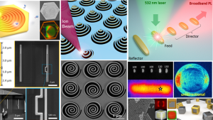
Nanotechnology, Synthetic Materials, Metasurfaces, and Photonic Integrated Circuits.
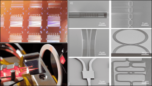
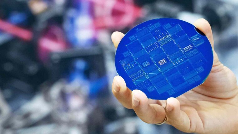
Nanostructured silicon wafer with a set of photonic integrated circuits for photonic information processing
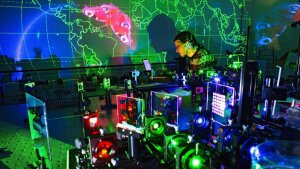
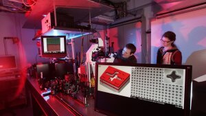
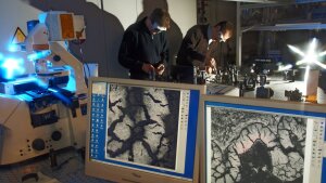
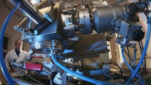
The ACP key research area Nanophotonics & Photonic Materials explore the interaction of light with nanometer-scale structures and advanced materials to revolutionize optical technologies. This field integrates Nanotechnology and Synthetic Materials to design and fabricate highly functional photonic components, including Metasurfaces, which manipulate light in novel ways for applications in imaging, sensing, and communication. Photonic Integrated Circuits (PICs) enable the miniaturization and integration of photonic devices, driving the development of faster, more efficient systems for data processing and telecommunications.
