Atomic Layer Deposition
Dr. Adriana SZEGHALMI

Email: a.szeghalmi@uni-jena.de, adriana.szeghalmi@iof.fraunhofer.de
Phone: +49 3641-9-47859
Dr. Adriana Szeghalmi is head of the research group Atomic Layer Deposition of Optical Coatings and of the ATTRACT research group Atomic Layer Deposition for Optics at the Fraunhofer Institute for Applied Optics and Precision Engineering (IOF) Jena.
The Atomic Layer Deposition Group aims to establish this technology for the development of novel and improved optical elements. We currently focus on devel-oping atomic layer deposited coatings for:
Dr. Szeghalmi currently mentors three doctoral students and a postdoctoral scientist. Graduate students interested in handson experience in optical coatings and optical design are welcome to join the group. A course on inorganic and organic materials in photonics is in preparation.
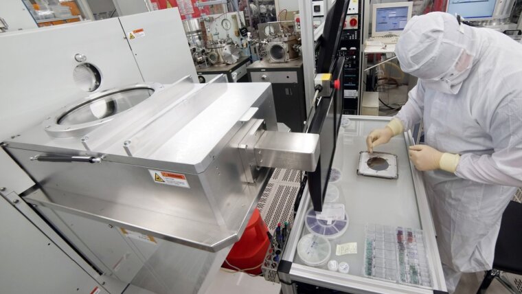
The ALD facility led by Dr. Szeghalmi has two plasmaenhanced atomic layer deposition reactors at hand. Both are located in a clean room environment and are equipped with in situ monitoring techniques for experimental characterization by means of spectroscopic ellipsometry in the 245 nm to 1700 nm spectral range. The equipment comprises:
Atomic layer deposition (ALD) is a cyclic, self-limiting chemical deposition technique. The thickness of ALD films is controlled with sub-nanometer precision by the number of ALD cycles. The films manifest high uniformity and low roughness. Most importantly, conformal coating can be achieved on nanostructured materials. A wide range of materials, including oxides, nitrides, fluorides, sulfides, metals and hybrid organic-inorganic composites, can be deposited via the ALD and molecular layer deposition (MLD) techniques. The above-mentioned materials find numerous applications in the fields of photovoltaics, electronics, catalysis, biotechnology, display technology, and photonics.
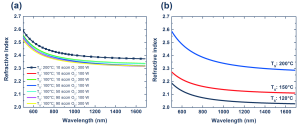
High and low refractive index dielectrics are essential for refractive and diffractive optics. High optical quality and excellent reproducibility have been achieved for SiO2, Al2O3, HfO2, Ta2O5, and TiO2 coatings. The deposition of titanium dioxide (TiO2) using/via ALD was thoroughly investigated [1] and the optical properties are depicted in Figure 1.
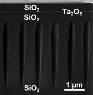
Encapsulated gratings show higher efficiency levels than do binary gratings. An improved encapsulation process was developed based on atomic layer deposition and microstructuring. A detailed description of the process is published in [2]. Figure 2 shows a cross-sectioned FIBSEM image of an encapsulated grating designed for TM-polarized light at wavelengths of 1000…1064 nm. The first SiO2 layer on top of the grating is realized via/using ALD deposition to ensure a high degree of chem-ical bonding to the substrate. Fortunately, no boundary is visible between the grating top and the encapsulation layer. The Ta2O5 and SiO2 layers serve as antireflection coatings made via PVD. The system is in accordance with the ISO:9211-4:2007-03 norm pertaining to the adhesive strength of the layers. The grating efficiency is 97.5% at 1030 nm. The encapsulated grating has a much higher efficiency (up to 8%) than conventional binary gratings in the given spectral range.
[1] Ratzsch et al., Nanotechnol., 26, 11 (2015).
[2] Ratzsch et al., Opt. Express, 23, 17955 (2015).